
之前在比赛准备的时候有准备过关于锁相环相关的器件,这里介绍一下ADF4351这款宽带频率合成器的使用。
由于我使用的是购买来的成品模块,所以这里着重讲的是软件驱动方面。
首先根据手册可以看到,这是一款35MHz到4.4GHz的锁相环芯片,具有低相位噪声等优点,同时支持小数和整数分频。其实它的VCO是2.2GHz到4.4GHz的振荡器,其余35MHz到2.2GHz全部是由可编程的输出分频器分频得到的。这款芯片的性能是非常好的,输出的信号相位噪声很低,手册上给出的数据是−100dBc/Hz 3 kHz from 2111.28 MHz carrier,在实际测试中发现我手中的这块芯片甚至略微超出了这个参数。
接下来关注到,其配置方式是通过一个3-wire的串行总线完成的,那么可以关注一下这个总线的通信时序: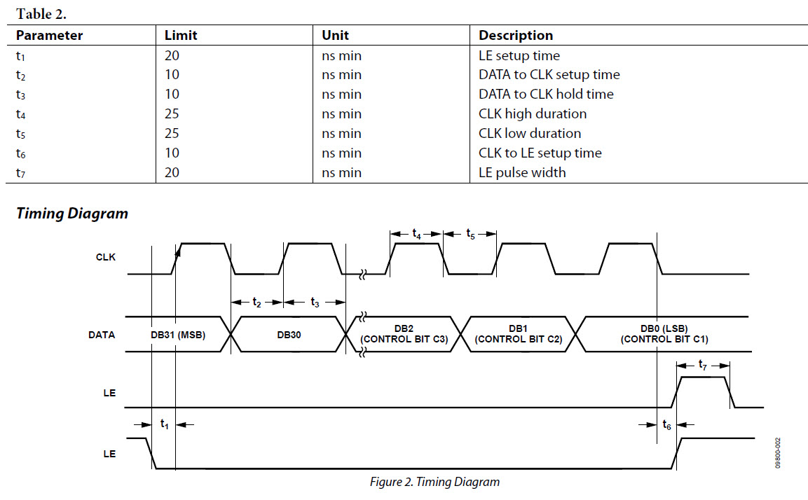
从时序可以看出,这个三线串口中,有一条使能线,一条时钟线和一条数据线,这个三线串口其实就是SPI接口,所以我们可以直接调用单片机的硬件SPI模块来与其通信。并且需要注意的是,在这个协议当中,后三位表示的是寄存器的编号,而且这个协议的速率不应该高于20Mbps。
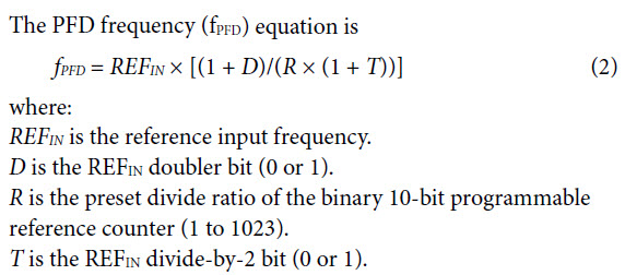
关于如何配置这块芯片,就需要大致的了解一下它的工作原理。首先向其输入一个REF-in的参考输入信号,然后这个参考信号在通过一个缓冲器之后,会进入一个名为R counter的计数器中,这里呢就使用了计数器对输入的参考信号进行分频,这一步的分频可以使得分频后的信号拥有更小的相位噪声。同时,由压控振荡器VCO产生的信号经过N counter计数器后,一并通入鉴频鉴相器中。最后将鉴频鉴相器的输入通入电荷泵,通过电荷泵后的电压再用来控制VCO。所以输出频率的计算公式即为:
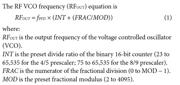
但是需要注意的是,RF_OUT的值必须是一个2.2G到4.4G之间的值,因为它是压控振荡器VCO的输出值。而最终芯片的输出频率35MHz-4.4GHz需要将RF_OUT的输出值再进行一个2的次方倍分频才行。
关于寄存器的功能,便不再详述,手册上写的非常详尽。
最后附上代码(双击代码区域复制):
/**
  ******************************************************************************
  * File Name          : main.c
  * Description        : Main program body
  ******************************************************************************
  *
  * COPYRIGHT(c) 2017 STMicroelectronics
  *
  * Redistribution and use in source and binary forms, with or without modification,
  * are permitted provided that the following conditions are met:
  *   1. Redistributions of source code must retain the above copyright notice,
  *      this list of conditions and the following disclaimer.
  *   2. Redistributions in binary form must reproduce the above copyright notice,
  *      this list of conditions and the following disclaimer in the documentation
  *      and/or other materials provided with the distribution.
  *   3. Neither the name of STMicroelectronics nor the names of its contributors
  *      may be used to endorse or promote products derived from this software
  *      without specific prior written permission.
  *
  * THIS SOFTWARE IS PROVIDED BY THE COPYRIGHT HOLDERS AND CONTRIBUTORS "AS IS"
  * AND ANY EXPRESS OR IMPLIED WARRANTIES, INCLUDING, BUT NOT LIMITED TO, THE
  * IMPLIED WARRANTIES OF MERCHANTABILITY AND FITNESS FOR A PARTICULAR PURPOSE ARE
  * DISCLAIMED. IN NO EVENT SHALL THE COPYRIGHT HOLDER OR CONTRIBUTORS BE LIABLE
  * FOR ANY DIRECT, INDIRECT, INCIDENTAL, SPECIAL, EXEMPLARY, OR CONSEQUENTIAL
  * DAMAGES (INCLUDING, BUT NOT LIMITED TO, PROCUREMENT OF SUBSTITUTE GOODS OR
  * SERVICES; LOSS OF USE, DATA, OR PROFITS; OR BUSINESS INTERRUPTION) HOWEVER
  * CAUSED AND ON ANY THEORY OF LIABILITY, WHETHER IN CONTRACT, STRICT LIABILITY,
  * OR TORT (INCLUDING NEGLIGENCE OR OTHERWISE) ARISING IN ANY WAY OUT OF THE USE
  * OF THIS SOFTWARE, EVEN IF ADVISED OF THE POSSIBILITY OF SUCH DAMAGE.
  *
  ******************************************************************************
  */
/* Includes ------------------------------------------------------------------*/
#include "main.h"
#include "stm32f1xx_hal.h"

/* USER CODE BEGIN Includes */

/* USER CODE END Includes */

/* Private variables ---------------------------------------------------------*/
CRC_HandleTypeDef hcrc;

IWDG_HandleTypeDef hiwdg;

SPI_HandleTypeDef hspi2;

TIM_HandleTypeDef htim6;
TIM_HandleTypeDef htim7;

WWDG_HandleTypeDef hwwdg;

/* USER CODE BEGIN PV */
/* Private variables ---------------------------------------------------------*/
#define PLL_PROT hspi2
typedef struct PLL_Configure{
    enum{
        PLL_DISABLE = 0,
        PLL_ENABLE
    };
    unsigned short integer_value;						//16-bit Greater than 23, to 65535
    unsigned short fractional_value;				//12-bit 0 to 4095
    unsigned char phase_adjust;							//1-bit 0-OFF 1-ON
    enum{
        PHASE_ADJ_OFF = 0,
        PHASE_ADJ_ON
    }phase_adjust_type;
    //unsigned char prescaler;								//1-bit 0-(4/5) 1-(8/9)
    enum prescaler_type{
        PRESCALER_4Div5 = 0,
        PRESCALER_8Div9
    }prescaler;
    //enum prescaler_type prescaler;
    unsigned short phase_value;							//12-bit 0 to 4095, 1 is recommended
    unsigned short modulus_value;						//12-bit Greater than 2, to 4095
    unsigned char low_noise_and_low_spur;		//2-bit 00b-(Low Noise Mode) 11b-(Low Spur Mode)
    enum{
        LOW_NOISE = 0,
        LOW_SUPR = 3
    }low_nose_and_low_spur_type;
    unsigned char muxout;										//3-bit
    enum{
        MUXOUT_Three_State_Output = 0,
        MUXOUT_DVdd,
        MUXOUT_DGND,
        MUXOUT_R_COUNTER,
        MUXOUT_N_DIVIDER,
        MUXOUT_ANALOG_LOCK_DETECT,
        MUXOUT_DIGITAL_LOCK_DETECT,
        MUXOUT_RESERVED
    }muxout_type;
    //000b-Three-State Output
    //001b-DVdd
    //010b-DGND
    //011b-R Counter Output
    //100b-N Divider Output
    //101b-Analog Lock Detect
    //110b-Digital Lock Detect
    //111b-Reserved
    unsigned char reference_doubler;				//1-bit 0-Disable 1-Enable
    unsigned char reference_divide_by2;			//1-bit 0-Disable 1-Enable
    unsigned short r_counter;								//10-bit Greater than 1, to 1023
    unsigned char double_buffer;						//1-bit 0-Disable 1-Enable
    unsigned char charge_pump_current;			//4-bit 0 to 15
    /*CHARGE PUMP CURRENT SETTING VALUE
    0000 0.31
    0001 0.63
    0010 0.94
    0011 1.25
    0100 1.56
    0101 1.88
    0110 2.19
    0111 2.50
    1000 2.81
    1001 3.13
    1010 3.44
    1011 3.75
    1100 4.06
    1101 4.38
    1110 4.69
    1111 5.00*/
    unsigned char LDF;											//1-bit 0-FRAC-N 1-INT-N
    enum{
        FRAC_N = 0,
        INT_N
    }LDF_type;
    unsigned char LDP;											//1-bit 0-10ns 1-6ns
    enum{
        LDP_10ns = 0,
        LDP_6ns
    }LDP_type;
    unsigned char PD_polarity;							//1-bit 0-NEGTIVE 1-POSITIVE
    enum{
        NEGTIVE = 0,
        POSITIVE
    }PD_polarity_type;
    unsigned char power_down;								//1-bit 0-Disable 1-Enable
    unsigned char CP_three_state;						//1-bit 0-Disable 1-Enable
    unsigned char counter_reset;						//1-bit 0-Disable 1-Enable
    unsigned char band_select_clock;				//1-bit 0-LOW 1-HIGH
    enum{
        LOW = 0,
        HIGH
    }band_select_clock_type;
    unsigned char antibacklash_pulse_width;	//1-bit 0-6ns 1-3ns
    enum{
        ANTIBACKLASH_PULSE_6ns = 0,
        ANTIBACKLASH_PULSE_3ns
    }antibacklash_pulse_type;
    unsigned char charge_cancelation;				//1-bit 0-Disable 1-Enable
    unsigned char cycle_slip_reduction;			//1-bit 0-Disable	1-Enable
    unsigned char clk_div_mode;							//2-bit
    enum{
        CLOCK_DIVIDER_OFF = 0,
        FAST_LOCK_ENABLE,
        RESYNC_ENABLE
    }clk_div_mode_type;
    unsigned short clock_divider_value;			//12-bit 0 to 4095
    unsigned char feedback_select;					//1-bit 0-Divided 1-Fundamental
    enum{
        DIVIDED = 0,
        FUNDAMENTAL
    }feedback_select_type;
    unsigned char RF_divider_select;				//3-bit
    /*RF DIVIDER SELECT
    000 /1
    001 /2
    010 /4
    011 /8
    100 /16
    101 /32
    110 /64
    */
    unsigned char band_select_clock_divider;//8-bit Greater than 1, to 255
    unsigned char VCO_power_down;						//1-bit 0-Power Up 1-Power Down
    enum{
        VCO_POWER_UP = 0,
        VCO_POWER_DOWN
    }VCO_power_down_type;
    unsigned char mute_till_lock_detect;		//1-bit 0-Mute Disable 1-Mute Enable
    enum{
        MUTE_DISABLE = 0,
        MUTE_ENABLE
    }mute_till_lock_detect_type;
    unsigned char AUX_output_select;				//1-bit 0-Divided Output 1-Fundamental
    enum{
        DIVIDED_OUTPUTE = 0
        //FUNDAMENTAL
    }AUX_output_select_type;
    unsigned char AUX_output;								//1-bit 0-Disable 1-Enable
    unsigned char AUX_output_power;					//2-bit 0 to 3
    /*AUX OUTPUT POWER
    00 -4dBm
    01 -1dBm
    10 +2dBm
    11 +5dBm
    */
    unsigned char RF_OUT;										//1-bit 0-Disable 1-Enable
    unsigned char output_power;							//2-bit
    /*OUTPUT POWER
    00 -4dBm
    01 -1dBm
    10 +2dBm
    11 +5dBm
    */
    unsigned char LD_pin_mode;							//2-bit
    enum{
        LD_LOW = 0,
        DIGITAL_LOCK_DETECT,
        //LOW,
        LD_HIGH = 3
    }LD_pin_mode_type;
}PLL_CFG;
/* USER CODE END PV */

/* Private function prototypes -----------------------------------------------*/
void SystemClock_Config(void);
void Error_Handler(void);
static void MX_GPIO_Init(void);
static void MX_CRC_Init(void);
static void MX_IWDG_Init(void);
static void MX_TIM6_Init(void);
static void MX_TIM7_Init(void);
static void MX_WWDG_Init(void);
static void MX_SPI2_Init(void);
static void MX_NVIC_Init(void);

/* USER CODE BEGIN PFP */
/* Private function prototypes -----------------------------------------------*/
void PLL_Config(PLL_CFG *config);
void PLL_Init(void);
void PLL_Enable(void);
void PLL_Disable(void);
void PLL_RF_Enable(void);
void PLL_RF_Disable(void);
/* USER CODE END PFP */

/* USER CODE BEGIN 0 */

/* USER CODE END 0 */

int main(void)
{

  /* USER CODE BEGIN 1 */
    char a = 0;
  /* USER CODE END 1 */

  /* MCU Configuration----------------------------------------------------------*/

  /* Reset of all peripherals, Initializes the Flash interface and the Systick. */
  HAL_Init();

  /* Configure the system clock */
  SystemClock_Config();

  /* Initialize all configured peripherals */
  MX_GPIO_Init();
  MX_CRC_Init();
  MX_IWDG_Init();
  MX_TIM6_Init();
  MX_TIM7_Init();
  MX_WWDG_Init();
  MX_SPI2_Init();

  /* Initialize interrupts */
  MX_NVIC_Init();

  /* USER CODE BEGIN 2 */
    HAL_Delay(500);
    PLL_Init();
  /* USER CODE END 2 */

  /* Infinite loop */
  /* USER CODE BEGIN WHILE */
  while (1)
  {
  /* USER CODE END WHILE */

  /* USER CODE BEGIN 3 */
  }
  /* USER CODE END 3 */

}

/** System Clock Configuration
*/
void SystemClock_Config(void)
{

  RCC_OscInitTypeDef RCC_OscInitStruct;
  RCC_ClkInitTypeDef RCC_ClkInitStruct;

    /**Initializes the CPU, AHB and APB busses clocks
    */
  RCC_OscInitStruct.OscillatorType = RCC_OSCILLATORTYPE_LSI|RCC_OSCILLATORTYPE_HSE;
  RCC_OscInitStruct.HSEState = RCC_HSE_ON;
  RCC_OscInitStruct.HSEPredivValue = RCC_HSE_PREDIV_DIV1;
  RCC_OscInitStruct.HSIState = RCC_HSI_ON;
  RCC_OscInitStruct.LSIState = RCC_LSI_ON;
  RCC_OscInitStruct.PLL.PLLState = RCC_PLL_ON;
  RCC_OscInitStruct.PLL.PLLSource = RCC_PLLSOURCE_HSE;
  RCC_OscInitStruct.PLL.PLLMUL = RCC_PLL_MUL9;
  if (HAL_RCC_OscConfig(&RCC_OscInitStruct) != HAL_OK)
  {
    Error_Handler();
  }

    /**Initializes the CPU, AHB and APB busses clocks
    */
  RCC_ClkInitStruct.ClockType = RCC_CLOCKTYPE_HCLK|RCC_CLOCKTYPE_SYSCLK
                              |RCC_CLOCKTYPE_PCLK1|RCC_CLOCKTYPE_PCLK2;
  RCC_ClkInitStruct.SYSCLKSource = RCC_SYSCLKSOURCE_PLLCLK;
  RCC_ClkInitStruct.AHBCLKDivider = RCC_SYSCLK_DIV1;
  RCC_ClkInitStruct.APB1CLKDivider = RCC_HCLK_DIV2;
  RCC_ClkInitStruct.APB2CLKDivider = RCC_HCLK_DIV1;

  if (HAL_RCC_ClockConfig(&RCC_ClkInitStruct, FLASH_LATENCY_2) != HAL_OK)
  {
    Error_Handler();
  }

    /**Configure the Systick interrupt time
    */
  HAL_SYSTICK_Config(HAL_RCC_GetHCLKFreq()/1000);

    /**Configure the Systick
    */
  HAL_SYSTICK_CLKSourceConfig(SYSTICK_CLKSOURCE_HCLK);

  /* SysTick_IRQn interrupt configuration */
  HAL_NVIC_SetPriority(SysTick_IRQn, 0, 0);
}

/** NVIC Configuration
*/
static void MX_NVIC_Init(void)
{
  /* EXTI9_5_IRQn interrupt configuration */
  HAL_NVIC_SetPriority(EXTI9_5_IRQn, 0, 0);
  HAL_NVIC_EnableIRQ(EXTI9_5_IRQn);
  /* EXTI15_10_IRQn interrupt configuration */
  HAL_NVIC_SetPriority(EXTI15_10_IRQn, 0, 0);
  HAL_NVIC_EnableIRQ(EXTI15_10_IRQn);
  /* SPI2_IRQn interrupt configuration */
  HAL_NVIC_SetPriority(SPI2_IRQn, 0, 0);
  HAL_NVIC_EnableIRQ(SPI2_IRQn);
}

/* CRC init function */
static void MX_CRC_Init(void)
{

  hcrc.Instance = CRC;
  if (HAL_CRC_Init(&hcrc) != HAL_OK)
  {
    Error_Handler();
  }

}

/* IWDG init function */
static void MX_IWDG_Init(void)
{

  hiwdg.Instance = IWDG;
  hiwdg.Init.Prescaler = IWDG_PRESCALER_4;
  hiwdg.Init.Reload = 4095;
  if (HAL_IWDG_Init(&hiwdg) != HAL_OK)
  {
    Error_Handler();
  }

}

/* SPI2 init function */
static void MX_SPI2_Init(void)
{

  hspi2.Instance = SPI2;
  hspi2.Init.Mode = SPI_MODE_MASTER;
  hspi2.Init.Direction = SPI_DIRECTION_2LINES;
  hspi2.Init.DataSize = SPI_DATASIZE_16BIT;
  hspi2.Init.CLKPolarity = SPI_POLARITY_LOW;
  hspi2.Init.CLKPhase = SPI_PHASE_1EDGE;
  hspi2.Init.NSS = SPI_NSS_SOFT;
  hspi2.Init.BaudRatePrescaler = SPI_BAUDRATEPRESCALER_2;
  hspi2.Init.FirstBit = SPI_FIRSTBIT_MSB;
  hspi2.Init.TIMode = SPI_TIMODE_DISABLE;
  hspi2.Init.CRCCalculation = SPI_CRCCALCULATION_DISABLE;
  hspi2.Init.CRCPolynomial = 10;
  if (HAL_SPI_Init(&hspi2) != HAL_OK)
  {
    Error_Handler();
  }

}

/* TIM6 init function */
static void MX_TIM6_Init(void)
{

  TIM_MasterConfigTypeDef sMasterConfig;

  htim6.Instance = TIM6;
  htim6.Init.Prescaler = 0;
  htim6.Init.CounterMode = TIM_COUNTERMODE_UP;
  htim6.Init.Period = 0;
  if (HAL_TIM_Base_Init(&htim6) != HAL_OK)
  {
    Error_Handler();
  }

  sMasterConfig.MasterOutputTrigger = TIM_TRGO_RESET;
  sMasterConfig.MasterSlaveMode = TIM_MASTERSLAVEMODE_DISABLE;
  if (HAL_TIMEx_MasterConfigSynchronization(&htim6, &sMasterConfig) != HAL_OK)
  {
    Error_Handler();
  }

}

/* TIM7 init function */
static void MX_TIM7_Init(void)
{

  TIM_MasterConfigTypeDef sMasterConfig;

  htim7.Instance = TIM7;
  htim7.Init.Prescaler = 0;
  htim7.Init.CounterMode = TIM_COUNTERMODE_UP;
  htim7.Init.Period = 0;
  if (HAL_TIM_Base_Init(&htim7) != HAL_OK)
  {
    Error_Handler();
  }

  sMasterConfig.MasterOutputTrigger = TIM_TRGO_RESET;
  sMasterConfig.MasterSlaveMode = TIM_MASTERSLAVEMODE_DISABLE;
  if (HAL_TIMEx_MasterConfigSynchronization(&htim7, &sMasterConfig) != HAL_OK)
  {
    Error_Handler();
  }

}

/* WWDG init function */
static void MX_WWDG_Init(void)
{

  hwwdg.Instance = WWDG;
  hwwdg.Init.Prescaler = WWDG_PRESCALER_1;
  hwwdg.Init.Window = 64;
  hwwdg.Init.Counter = 64;
  if (HAL_WWDG_Init(&hwwdg) != HAL_OK)
  {
    Error_Handler();
  }

}

/** Configure pins as
        * Analog
        * Input
        * Output
        * EVENT_OUT
        * EXTI
*/
static void MX_GPIO_Init(void)
{

  GPIO_InitTypeDef GPIO_InitStruct;

  /* GPIO Ports Clock Enable */
  __HAL_RCC_GPIOC_CLK_ENABLE();
  __HAL_RCC_GPIOD_CLK_ENABLE();
  __HAL_RCC_GPIOA_CLK_ENABLE();
  __HAL_RCC_GPIOB_CLK_ENABLE();

  /*Configure GPIO pin Output Level */
  HAL_GPIO_WritePin(GPIOA, PLL_EN_Pin|RF_OUT_EN_Pin, GPIO_PIN_RESET);

  /*Configure GPIO pin Output Level */
  HAL_GPIO_WritePin(Load_Enable_GPIO_Port, Load_Enable_Pin, GPIO_PIN_SET);

  /*Configure GPIO pin Output Level */
  HAL_GPIO_WritePin(LED0_GPIO_Port, LED0_Pin, GPIO_PIN_SET);

  /*Configure GPIO pin Output Level */
  HAL_GPIO_WritePin(LED1_GPIO_Port, LED1_Pin, GPIO_PIN_SET);

  /*Configure GPIO pins : PLL_EN_Pin RF_OUT_EN_Pin LED0_Pin */
  GPIO_InitStruct.Pin = PLL_EN_Pin|RF_OUT_EN_Pin|LED0_Pin;
  GPIO_InitStruct.Mode = GPIO_MODE_OUTPUT_PP;
  GPIO_InitStruct.Speed = GPIO_SPEED_FREQ_HIGH;
  HAL_GPIO_Init(GPIOA, &GPIO_InitStruct);

  /*Configure GPIO pin : Load_Enable_Pin */
  GPIO_InitStruct.Pin = Load_Enable_Pin;
  GPIO_InitStruct.Mode = GPIO_MODE_OUTPUT_PP;
  GPIO_InitStruct.Speed = GPIO_SPEED_FREQ_HIGH;
  HAL_GPIO_Init(Load_Enable_GPIO_Port, &GPIO_InitStruct);

  /*Configure GPIO pin : Digit_Lock_Detect_Pin */
  GPIO_InitStruct.Pin = Digit_Lock_Detect_Pin;
  GPIO_InitStruct.Mode = GPIO_MODE_IT_RISING_FALLING;
  GPIO_InitStruct.Pull = GPIO_NOPULL;
  HAL_GPIO_Init(Digit_Lock_Detect_GPIO_Port, &GPIO_InitStruct);

  /*Configure GPIO pin : Analog_Lock_Detect_Pin */
  GPIO_InitStruct.Pin = Analog_Lock_Detect_Pin;
  GPIO_InitStruct.Mode = GPIO_MODE_IT_RISING_FALLING;
  GPIO_InitStruct.Pull = GPIO_NOPULL;
  HAL_GPIO_Init(Analog_Lock_Detect_GPIO_Port, &GPIO_InitStruct);

  /*Configure GPIO pin : LED1_Pin */
  GPIO_InitStruct.Pin = LED1_Pin;
  GPIO_InitStruct.Mode = GPIO_MODE_OUTPUT_PP;
  GPIO_InitStruct.Speed = GPIO_SPEED_FREQ_HIGH;
  HAL_GPIO_Init(LED1_GPIO_Port, &GPIO_InitStruct);

}

/* USER CODE BEGIN 4 */
void PLL_Enable(void)
{
    HAL_GPIO_WritePin(PLL_EN_GPIO_Port,PLL_EN_Pin,GPIO_PIN_SET);
}

void PLL_Disable(void)
{
    HAL_GPIO_WritePin(PLL_EN_GPIO_Port,PLL_EN_Pin,GPIO_PIN_RESET);
}

void PLL_RF_Enable(void)
{
    HAL_GPIO_WritePin(RF_OUT_EN_GPIO_Port,RF_OUT_EN_Pin,GPIO_PIN_SET);
}

void PLL_RF_Disable(void)
{
    HAL_GPIO_WritePin(RF_OUT_EN_GPIO_Port,RF_OUT_EN_Pin,GPIO_PIN_RESET);
}

void PLL_Config(PLL_CFG *config)
{
    uint32_t Reg[6];
    uint8_t i;
    Reg[0] &= 0x00000000;
    Reg[0] |= ((uint32_t)config->integer_value 						< < 15)	& 0x7FFF8000;
    Reg[0] |= ((uint32_t)config->fractional_value 				< < 3)		& 0x00007FF8;
    Reg[0] |= 0x00000000;
    Reg[1] &= 0x00000000;
    Reg[1] |= ((uint32_t)config->phase_adjust 						< < 28)	& 0x10000000;
    Reg[1] |= ((uint32_t)config->prescaler 								< < 27)	& 0x08000000;
    Reg[1] |= ((uint32_t)config->phase_value 							< < 15)	& 0x07FF8000;
    Reg[1] |= ((uint32_t)config->modulus_value 						< < 3)		& 0x00007FF8;
    Reg[1] |= 0x00000001;
    Reg[2] &= 0x00000000;
    Reg[2] |= ((uint32_t)config->low_noise_and_low_spur 	< < 29)	& 0x60000000;
    Reg[2] |= ((uint32_t)config->muxout 									< < 26)	& 0x1C000000;
    Reg[2] |= ((uint32_t)config->reference_doubler 				< < 25)	& 0x02000000;
    Reg[2] |= ((uint32_t)config->reference_divide_by2 		< < 24)	& 0x01000000;
    Reg[2] |= ((uint32_t)config->r_counter 								< < 14)	& 0x00FFC000;
    Reg[2] |= ((uint32_t)config->double_buffer 						< < 13)	& 0x00002000;
    Reg[2] |= ((uint32_t)config->charge_pump_current 			< < 9)		& 0x00001E00;
    Reg[2] |= ((uint32_t)config->LDF 											< < 8)		& 0x00000100;
    Reg[2] |= ((uint32_t)config->LDP 											< < 7)		& 0x00000080;
    Reg[2] |= ((uint32_t)config->PD_polarity 							< < 6)		& 0x00000040;
    Reg[2] |= ((uint32_t)config->power_down 							< < 5)		& 0x00000020;
    Reg[2] |= ((uint32_t)config->CP_three_state 					< < 4)		& 0x00000010;
    Reg[2] |= ((uint32_t)config->counter_reset 						< < 3)		& 0x00000008;
    Reg[2] |= 0x00000002;
    Reg[3] &= 0x00000000;
    Reg[3] |= ((uint32_t)config->band_select_clock 				< < 23)	& 0x00800000;
    Reg[3] |= ((uint32_t)config->antibacklash_pulse_width < < 22)	& 0x00400000;
    Reg[3] |= ((uint32_t)config->charge_cancelation				< < 21)	& 0x00200000;
    Reg[3] |= ((uint32_t)config->cycle_slip_reduction			< < 18)	& 0x00040000;
    Reg[3] |= ((uint32_t)config->clk_div_mode							< < 15)	& 0x00018000;
    Reg[3] |= ((uint32_t)config->clock_divider_value			< < 3)		& 0x00007FF8;
    Reg[3] |= 0x00000003;
    Reg[4] &= 0x00000000;
    Reg[4] |= ((uint32_t)config->feedback_select					< < 23)	& 0x00800000;
    Reg[4] |= ((uint32_t)config->RF_divider_select				< < 20)	& 0x00700000;
    Reg[4] |= ((uint32_t)config->band_select_clock_divider< < 12)	& 0x000FF000;
    Reg[4] |= ((uint32_t)config->VCO_power_down						< < 11)	& 0x00000800;
    Reg[4] |= ((uint32_t)config->mute_till_lock_detect		< < 10)	& 0x00000400;
    Reg[4] |= ((uint32_t)config->AUX_output_select				< < 9)		& 0x00000200;
    Reg[4] |= ((uint32_t)config->AUX_output								< < 8)		& 0x00000100;
    Reg[4] |= ((uint32_t)config->AUX_output_power					< < 6)		& 0x000000C0;
    Reg[4] |= ((uint32_t)config->RF_OUT										< < 5)		& 0x00000020;
    Reg[4] |= ((uint32_t)config->output_power							< < 3)		& 0x00000018;
    Reg[4] |= 0x00000004;
    Reg[5] &= 0x00000000;
    Reg[5] |= ((uint32_t)config->LD_pin_mode							< < 22)	& 0x00C00000;
    Reg[5] |= 0x00180000;
    Reg[5] |= 0x00000005;
    for(i=0;i<6;i++)
    {
        Reg[i] = ((Reg[i] >> 16) & 0x0000FFFF) | ((Reg[i] < < 16) & 0xFFFF0000);
    }
    HAL_GPIO_WritePin(Load_Enable_GPIO_Port,Load_Enable_Pin,GPIO_PIN_RESET);
    HAL_SPI_Transmit(&PLL_PROT,(uint8_t*)&Reg[5],2,1000);
    HAL_GPIO_WritePin(Load_Enable_GPIO_Port,Load_Enable_Pin,GPIO_PIN_SET);
    HAL_GPIO_WritePin(Load_Enable_GPIO_Port,Load_Enable_Pin,GPIO_PIN_RESET);
    HAL_SPI_Transmit(&PLL_PROT,(uint8_t*)&Reg[4],2,1000);
    HAL_GPIO_WritePin(Load_Enable_GPIO_Port,Load_Enable_Pin,GPIO_PIN_SET);
    HAL_GPIO_WritePin(Load_Enable_GPIO_Port,Load_Enable_Pin,GPIO_PIN_RESET);
    HAL_SPI_Transmit(&PLL_PROT,(uint8_t*)&Reg[3],2,1000);
    HAL_GPIO_WritePin(Load_Enable_GPIO_Port,Load_Enable_Pin,GPIO_PIN_SET);
    HAL_GPIO_WritePin(Load_Enable_GPIO_Port,Load_Enable_Pin,GPIO_PIN_RESET);
    HAL_SPI_Transmit(&PLL_PROT,(uint8_t*)&Reg[2],2,1000);
    HAL_GPIO_WritePin(Load_Enable_GPIO_Port,Load_Enable_Pin,GPIO_PIN_SET);
    HAL_GPIO_WritePin(Load_Enable_GPIO_Port,Load_Enable_Pin,GPIO_PIN_RESET);
    HAL_SPI_Transmit(&PLL_PROT,(uint8_t*)&Reg[1],2,1000);
    HAL_GPIO_WritePin(Load_Enable_GPIO_Port,Load_Enable_Pin,GPIO_PIN_SET);
    HAL_GPIO_WritePin(Load_Enable_GPIO_Port,Load_Enable_Pin,GPIO_PIN_RESET);
    HAL_SPI_Transmit(&PLL_PROT,(uint8_t*)&Reg[0],2,1000);
    HAL_GPIO_WritePin(Load_Enable_GPIO_Port,Load_Enable_Pin,GPIO_PIN_SET);
}

void PLL_Init(void)
{
    PLL_CFG PLL_InitStruct;
    PLL_InitStruct.integer_value = 22000;
    PLL_InitStruct.fractional_value = 0;
    //
    PLL_InitStruct.phase_adjust = PHASE_ADJ_OFF;
    PLL_InitStruct.prescaler = PRESCALER_8Div9;
    PLL_InitStruct.phase_value = 0;
    PLL_InitStruct.modulus_value = 2;
    //
    PLL_InitStruct.low_noise_and_low_spur = LOW_NOISE;
    PLL_InitStruct.muxout = MUXOUT_ANALOG_LOCK_DETECT;
    PLL_InitStruct.reference_doubler = ENABLE;
    PLL_InitStruct.reference_divide_by2 = ENABLE;
    PLL_InitStruct.r_counter = 250;
    PLL_InitStruct.double_buffer = DISABLE;
    PLL_InitStruct.charge_pump_current = 7;
    PLL_InitStruct.LDF = INT_N;
    PLL_InitStruct.LDP = LDP_10ns;
    PLL_InitStruct.PD_polarity = POSITIVE;
    PLL_InitStruct.power_down = DISABLE;
    PLL_InitStruct.CP_three_state = DISABLE;
    PLL_InitStruct.counter_reset = DISABLE;
    //
    PLL_InitStruct.band_select_clock = LOW;
    PLL_InitStruct.antibacklash_pulse_width = INT_N;
    PLL_InitStruct.cycle_slip_reduction = DISABLE;
    PLL_InitStruct.clk_div_mode = FAST_LOCK_ENABLE;
    PLL_InitStruct.clock_divider_value = 4;
    //
    PLL_InitStruct.feedback_select = FUNDAMENTAL;
    PLL_InitStruct.RF_divider_select = 6;
    PLL_InitStruct.band_select_clock_divider = 80;
    PLL_InitStruct.VCO_power_down = VCO_POWER_UP;
    PLL_InitStruct.mute_till_lock_detect = MUTE_ENABLE;
    PLL_InitStruct.AUX_output_select = DIVIDED_OUTPUTE;
    PLL_InitStruct.AUX_output = DISABLE;
    PLL_InitStruct.AUX_output_power = 0;
    PLL_InitStruct.RF_OUT = ENABLE;
    PLL_InitStruct.output_power = 5;
    //
    PLL_InitStruct.LD_pin_mode = DIGITAL_LOCK_DETECT;
    //
    PLL_Enable();
    PLL_Config(&PLL_InitStruct);
}

void HAL_GPIO_EXTI_Callback(uint16_t GPIO_Pin)
{
    GPIO_PinState tmp;
    switch(GPIO_Pin)
    {
        case Digit_Lock_Detect_Pin:
            tmp = HAL_GPIO_ReadPin(Digit_Lock_Detect_GPIO_Port,Digit_Lock_Detect_Pin);
            HAL_GPIO_WritePin(LED0_GPIO_Port,LED0_Pin,!tmp);
            if(tmp == GPIO_PIN_SET)
            {
                PLL_RF_Enable();
            }
            break;
        case Analog_Lock_Detect_Pin:
            tmp = HAL_GPIO_ReadPin(Analog_Lock_Detect_GPIO_Port,Analog_Lock_Detect_Pin);
            HAL_GPIO_WritePin(LED1_GPIO_Port,LED1_Pin,!tmp);
            break;
    }
}
/* USER CODE END 4 */

/**
  * @brief  This function is executed in case of error occurrence.
  * @param  None
  * @retval None
  */
void Error_Handler(void)
{
  /* USER CODE BEGIN Error_Handler */
  /* User can add his own implementation to report the HAL error return state */
  while(1)
  {
  }
  /* USER CODE END Error_Handler */
}

#ifdef USE_FULL_ASSERT

/**
   * @brief Reports the name of the source file and the source line number
   * where the assert_param error has occurred.
   * @param file: pointer to the source file name
   * @param line: assert_param error line source number
   * @retval None
   */
void assert_failed(uint8_t* file, uint32_t line)
{
  /* USER CODE BEGIN 6 */
  /* User can add his own implementation to report the file name and line number,
    ex: printf("Wrong parameters value: file %s on line %d\r\n", file, line) */
  /* USER CODE END 6 */

}

#endif

/**
  * @}
  */

/**
  * @}
*/

/************************ (C) COPYRIGHT STMicroelectronics *****END OF FILE****/
(完)